-
Applied Materials and CEA-Leti Unveil Joint Lab For Rapidly Growing Specialty Chip Markets
Source: Nasdaq GlobeNewswire / 05 Dec 2023 04:30:54 America/Los_Angeles
SANTA CLARA, Calif. and GRENOBLE, France, Dec. 05, 2023 (GLOBE NEWSWIRE) -- Applied Materials, Inc. and CEA-Leti today announced an expansion of their longstanding collaboration to focus on developing differentiated materials engineering solutions for several specialty semiconductor applications.
The joint lab, which represents CEA-Leti’s highest level of collaboration, aims to accelerate device innovations for Applied’s customers serving ICAPS markets (IoT, Communications, Automotive, Power and Sensors). Technology applications in those fields include photonics, image sensors, RF communications components, power devices and heterogeneous integration.
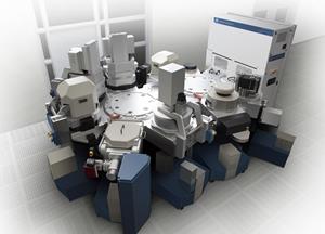
Demand for ICAPS applications and devices is being driven by industrial automation, the Internet of Things (IoT), electric vehicles, green energy and smart grid infrastructure, among other major high-growth markets. Projects at the joint lab will focus on developing solutions for a variety of materials engineering challenges to enable the next wave of ICAPS device innovation. The joint lab features several of Applied Materials’ 200mm and 300mm wafer processing systems and leverages CEA-Leti’s world-class capabilities for evaluating performance of new materials and device validation. Improvements in power consumption, performance and area/cost, along with faster time to market (PPACt™), will be key objectives of the joint team.
“CEA-Leti and Applied Materials aim to accelerate innovation and advance the roadmaps of a wide range of specialty semiconductor technologies,” said Aninda Moitra, corporate vice president and general manager of Applied Materials’ ICAPS business. “Our work at the joint lab builds upon more than a decade of successful collaboration and further strengthens our combined ability to enable faster time to innovation for ICAPS chipmakers.”
“For the past 10 years, Applied Materials and CEA-Leti have collaborated through multiple, specific joint development programs, which have set the stage for establishing our new joint lab,” said Sébastian Dauvé, the institute’s CEO. “Past projects included work in domains such as advanced metrology, materials for memory applications and optical devices, bonding techniques, materials deposition and film growth (PVD, CVD, ECD, Epitaxy) and chemical-mechanical planarization (CMP). Our results brought high value to both partners and to customers around the world, and we look forward to expanding our engagement with this new lab.”
“The joint lab, which is based at CEA-Leti, will host Applied Materials scientists and involve some of its latest-generation equipment,” Dauvé said. “In addition to developing differentiated technological solutions for Applied’s customers, the work performed at the joint lab will help overcome current technical hurdles in support of CEA-Leti’s internal R&D programs.”
About Applied Materials
Applied Materials, Inc. (Nasdaq: AMAT) is the leader in materials engineering solutions used to produce virtually every new chip and advanced display in the world. Our expertise in modifying materials at atomic levels and on an industrial scale enables customers to transform possibilities into reality. At Applied Materials, our innovations make possible a better future. Learn more at www.appliedmaterials.com.About CEA-Leti (France)
CEA-Leti, a technology research institute at CEA, is a global leader in miniaturization technologies enabling smart, energy-efficient and secure solutions for industry. Founded in 1967, CEA-Leti pioneers micro & nanotechnologies, tailoring differentiating applicative solutions for global companies, SMEs and startups. CEA-Leti tackles critical challenges in healthcare, energy and digital migration. From sensors to data processing and computing solutions, CEA-Leti’s multidisciplinary teams deliver solid expertise, leveraging world-class pre-industrialization facilities. With a staff of more than 2,000 talents, a portfolio of 3,200 patents, 11,000 sq. meters of cleanroom space and a clear IP policy, the institute is based in Grenoble, France, and has offices in Silicon Valley, Brussels and Tokyo. CEA-Leti has launched 75 startups and is a member of the Carnot Institutes network. Follow us on www.leti-cea.com and @CEA_Leti.Technological expertise
CEA has a key role in transferring scientific knowledge and innovation from research to industry. This high-level technological research is carried out in particular in electronic and integrated systems, from microscale to nanoscale. It has a wide range of industrial applications in the fields of transport, health, safety and telecommunications, contributing to the creation of high-quality and competitive products.For more information: www.cea.fr/english
Applied Materials Contacts
Ricky Gradwohl (U.S. editorial/media) +1 408.235.4676
Audrey Pariente (Europe editorial/media) +49 174 336 57 68
Michael Sullivan (financial community) +1 408.986.7977CEA-Leti Press Contact
Agency
Sarah-Lyle Dampoux
sldampoux@mahoneylyle.com
+33 6 74 93 23 47A photo accompanying this announcement is available at https://www.globenewswire.com/NewsRoom/AttachmentNg/751971cd-d1aa-47e6-83e1-6b83e5dff92e

